
User Guide of Acsip EK-AI7931HD Highly
Integrated Stamp Module
Introduction
1.1.General Description
AI7931HD is a highly integrated stamp module that features an ARM® Cortex-M33 application processor, a low power 1×1 802.11a/b/g/n/ax dual-band Wi-Fi subsystem, a Bluetooth v5.0 subsystem and a Power Management Unit (PMU). The Wi-Fi subsystem and a Bluetooth v5.0 subsystem offer feature-rich wireless connectivity at high standards, and deliver reliable, cost-effective throughput from an extended distance.
Optimized RF architecture and baseband algorithms provide superb performance and low power consumption.
AI7931HD is designed to support standard based features in the areas of security, quality of service and international regulations, giving end users the greatest performance any time and in any circumstance. The AI7931HD is based on ARM® Cortex-M33 with floating point microcontroller (MCU) including SRAM/ROM memory. The chip also supports rich peripheral interfaces, including UART, SDIO, I2C, SPI, I2S, and auxiliary ADC. These features are used to download and debug a project on EK-AI7931HD.
The front view of the EK-AI7931HD including AI7931HD stamp module and a FTDI debug board is shown in Figure 1.
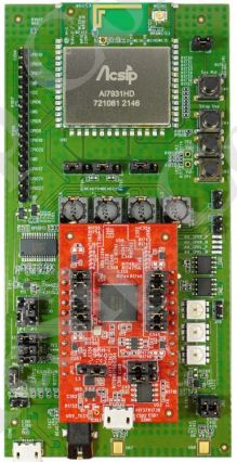
Figure 1. Front view of EK-AI7931HD and FTDI debug board
Get started with the HDK
Before commencing the application development, you need to configure the development platform.
2.1.Configuring the EK-AI7931HD
EK-AI7931HD includes a Base Board, a AI7931HD stamp module and a FTDI Debug board. The top view of the EK-AI7931HD is shown in Figure 2.
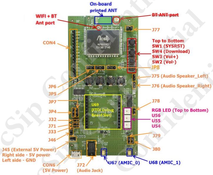
Figure 2. Jumpers and connectors on the EK-AI7931HD
The description of pins (Figure 2) and their functionality is provided below:
- CON6 is a USB 5V power for AI7931HD stamp module, or you can use external 5V power at J45.
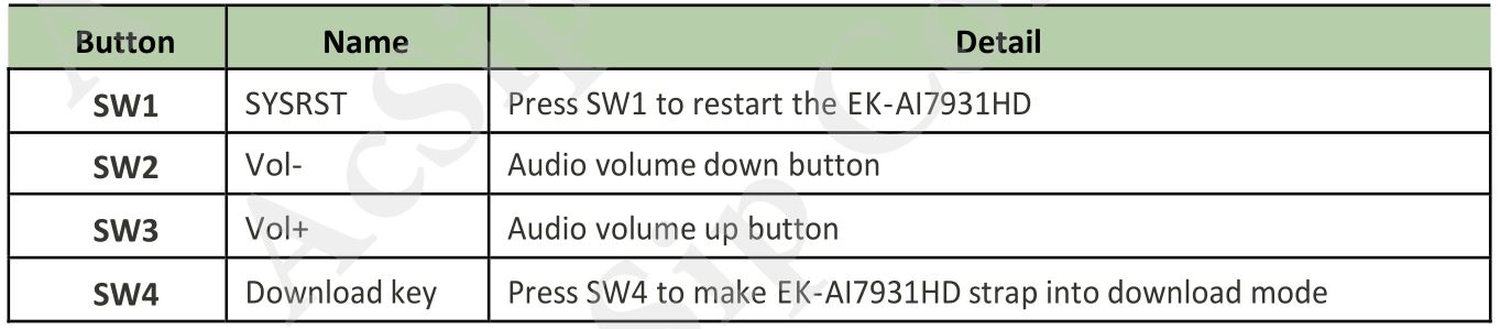
- Press SW1 to reset the system For SW2~SW4 more detail, please see “section 4.4”.
- For Wi-Fi and BT function AI7931HD stamp module reserve a Wi-Fi + BT RF-coaxial connector (MM8030-2610) and you can also use the on-board printed antenna to transmit and receive RF signal.
- The FTDI debug board can transfer USB interface to UART interface. Using this debug board can debug through UART,transmit, and receive a signal formPC.
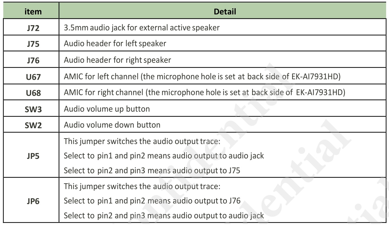
- U67 and U68 are on-board AMICs which can catch voice command.
- J75 and J76 are audio speaker connectors which can connect 8ohm/2W speaker to achieve voice assistant function.
- U54/U55/U56 are RGB LEDs and these RGB LED will be controlled by SPIM interface.
- CON4 support multifunction GPIO interface, for more detail please referto “section 4.7”.
2.2.Installing the FTDI debug board drivers on Microsoft Windows
To configure the EK-AI7931HD:
- Ensure the FTDI debug board insert to EK-AI7931HD at U69.
- Connect the FTDI debug board to the computer using a micro-USB cable.
- Connect a 5V power at EK-AI7931HD CON6 with a micro-USB cable.
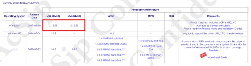
- Check your PC is X86 or X64 system and download and install FTDI Windows serial port driver from Here (The red block showed the download file at below figure).
- If your OS is Windows7 or 10, please open Windows Control Panel then click System and enter Device Manager.
- In Device Manager, navigate to Ports (COM & LPT) (see Figure 3).
- A new COM device should appear under Ports (COM & LPT)in Device Manager, as shown in Figure 3.
Note the COMx port number of the serial communication port, this information is needed to send command and receive logs from the COM port.
Due to the com port numbers (COMx) are different at different PC. In order to check the function of each com port we can recognize the order of these com ports as Figure 3 showed, the first com port (#1) means “DSP UART”, the second com port (#2) mean “UART0”, the third com port (#3) mean “UART1”, the fourth comport(#4) mean “CM33UART”.
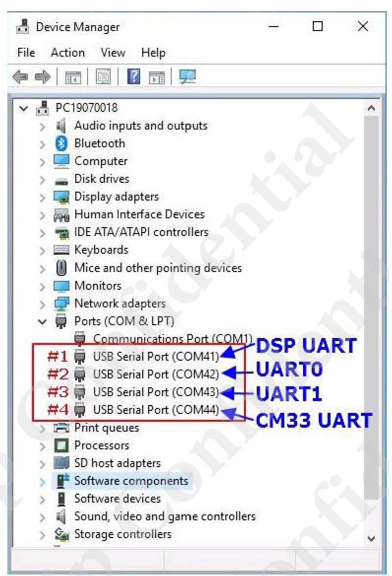
Figure 3. COM port associated with the EK-AI7931HD
Hardware Features
This section provides the main supported features of the EK-AI7931HD The detailed description of the features is provided in the upcoming sections
3.1.Features Description
3.1.1. Technology and Package
- AI7931HD Stamp Module: 30mm X 34mm X 2.7mm
3.1.2. Power Management and Clock Source
- Integrates high efficiency power management unit with single 3.3V power supply input.
- Integrates 26MHz crystal clock with low power operation in idle mode.
- Integrates 32KHz crystal oscillator for low power sleep mode.
3.1.3. Platform
- ARM® Cortex-M33 MCU with FPU with up to 300MHz clock speed.
- Embedded 1MB SRAM.
- Embedded 16MB serial flash with eXecute In Place (XIP) and on-the-fly AES.
- Supports Hardware crypto engines including AES, DES/3DES, SHA, ECC, TRNG for network security.
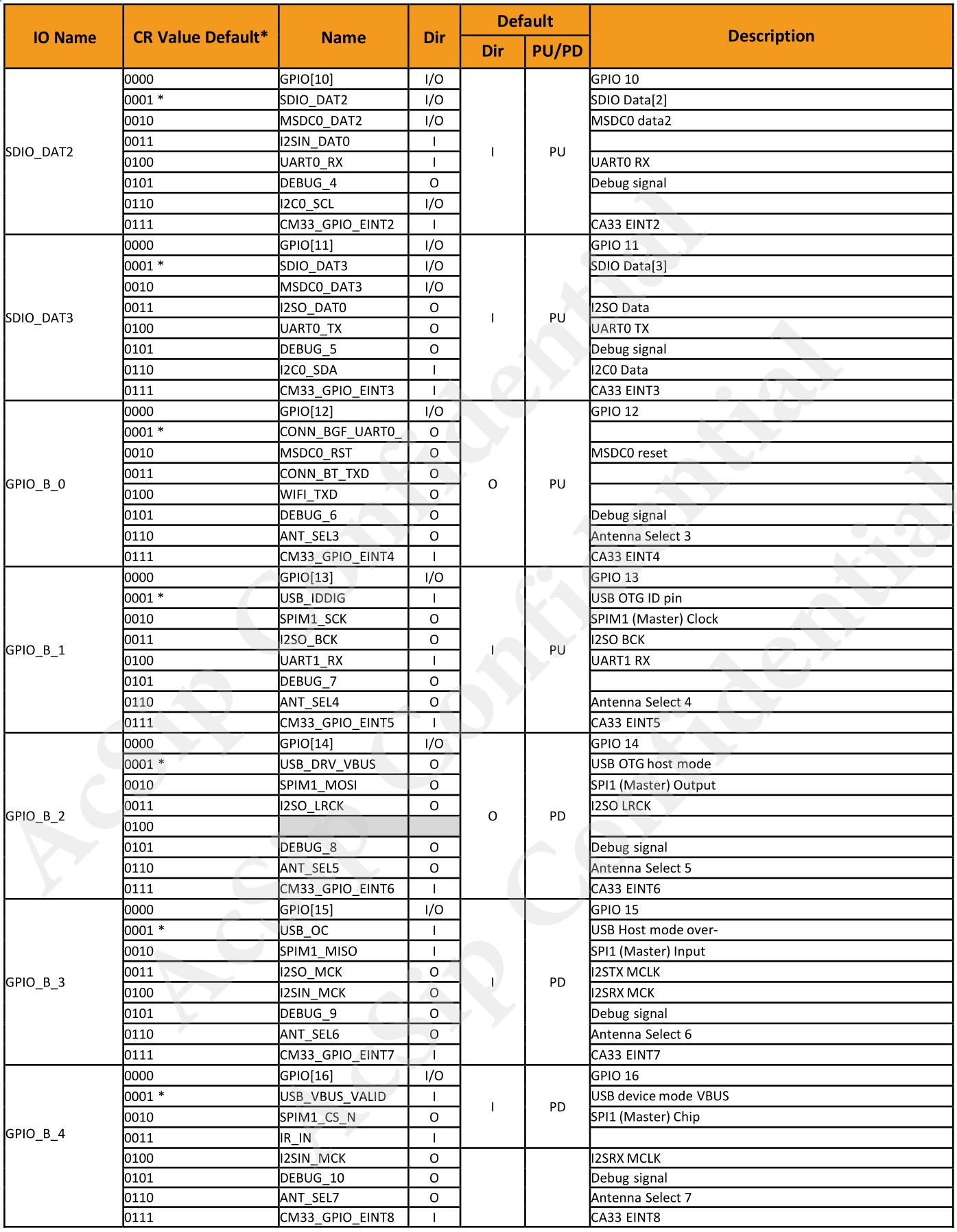
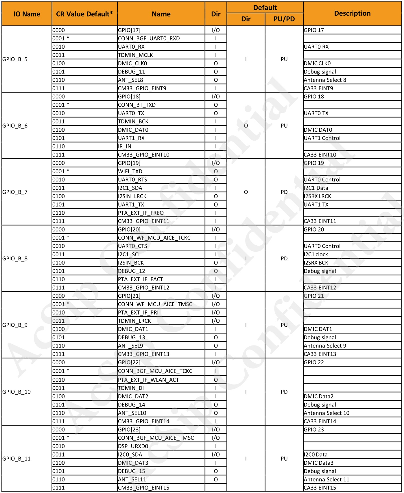
- Supports up to 22 General Purpose IOs, which are multiplexed with SPI, I2C, Aux ADC, UART, and GPIO interfaces.
- Supports 12 DMA channels.
3.1.4. Wi-Fi
- IEEE 802.11 1T1R a/b/g/n/ax 5GHz and 2.4GHz.
- Supports 20MHz, bandwidth in 2.4G/5GHz band, and MCS0~MCS8.
- Support uplink MU-OFDMA TX and downlink MU-OFDMA RX.
- Support STBC Rx, LDPC Tx, and RX Beamforming.
- Wi-Fi security WFA WPA/WPA2/WPA3 personal.
- Support 11ax TWT low power.
- Integrated balun, PA, LNA, and T/R switch.
- Support antenna diversity.
3.1.5. Bluetooth
- Bluetooth v5.0 with 2Mbps PHY rate, Long-range and LE Advertising Extensions
- Integrated balun and PA.
- Supports BT/Wi-Fi coexistence.
3.1.6. Miscellaneous
- Embedded eFuse to store specific device information and RF calibration data.
- Advanced TDD mode Wi-Fi/Bluetooth coexistence scheme.
Hardware Feature Configuration
4.1.Microcontroller
The MCU subsystem consists of a 32-bit MCU, the AHB/APB bus matrix, internal RAM/ROM with ROM patch function, the flash controller and the system peripherals including Direct Memory Access (DMA) engine and the General-Purpose Timer (GPT). The AI7931HD features an ARM® Cortex-M33 processor, which is the most energy efficient ARM® processor currently available. It supports the clock rates up to 200MHz when core power is 0.7V and 300MHz when core power is 0.8V.
The MCU executes the Thump-2 instruction set for optimal performance and code size, including hardware division, single cycle multiplication and bit-field manipulation. The AI7931HD includes a Memory Protection Unit (MPU) in Cortex-M33 MCU to detect unexpected memory access and provides other memory protection features. The AI7931HD also includes FPU in Cortex-M33 MCU.
4.2.Power supply
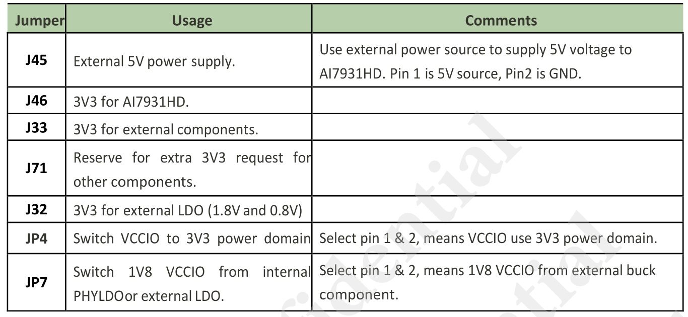
Power up with a micro-USB connector. An on-board switching regulator provides voltage of 3.3V for the EK-AI7931HD based on AI7931HD, if the power is supplied from an on-board micro-USB connector CON6 (Figure 2) Note, that the jumpers J46, J33, J32, JP4 pin2 and pin3 and JP7 pin2 and pin3 are required to be set on More details on the jumpers can be found in Table 1.
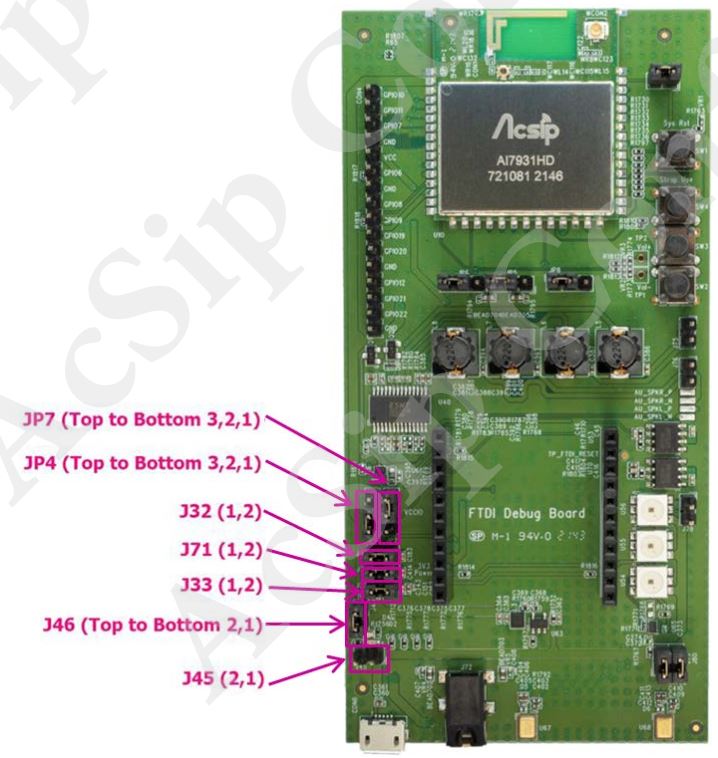
Figure 4. Default power jumper plot
Table 1 Jumper settings for system power input through USB connection
4.3. Audio
The EK-AI7931HD has on-board audio connector associated with different functionalities of the board.
The detail of audio related function can refer to Table 2.
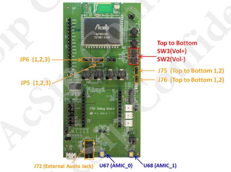
Figure 5. Audio related function
Table 2 Audio related function
4.4.Buttons
The EK-AI7931HD is equipped with buttons with the following functionality.
The push buttons are shown in Figure 2 The detail of buttons can refer to Table 3.
Table 3 Buttons
4.5.Antenna
By default, the board ships with RF signals routed to the on-board printed antenna. And AI7931HD reserve a conductive test component, (RF-coaxial connector, MM8030-2610) enables to test the signals using a compatible cable. Please refer to Figure 6 to see more detail.
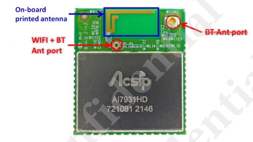
Figure 6. On-board printed antenna
4.6.RGB LED
As Figure7 showed, the EK-AI7931HD has on-board RGB LEDs (U54/U55/U56) which be controlled by SPIM interface. Please note that ensure jumper J79 and J80 are connected before using RGB LED function If you want to cascade more RGB LED, you can connect to J78
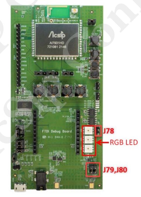
Figure 7. RGB LED
4.7.Extension connectors
The EK-AI7931HD provides similar pin-out extension connectors for various sensor and device connectivity, as shown in Figure 8 and described in Table 4.
The board has 13 GPIOs multiplexed with other interfaces. Depending on the use case, user can configure each I/O functionality.
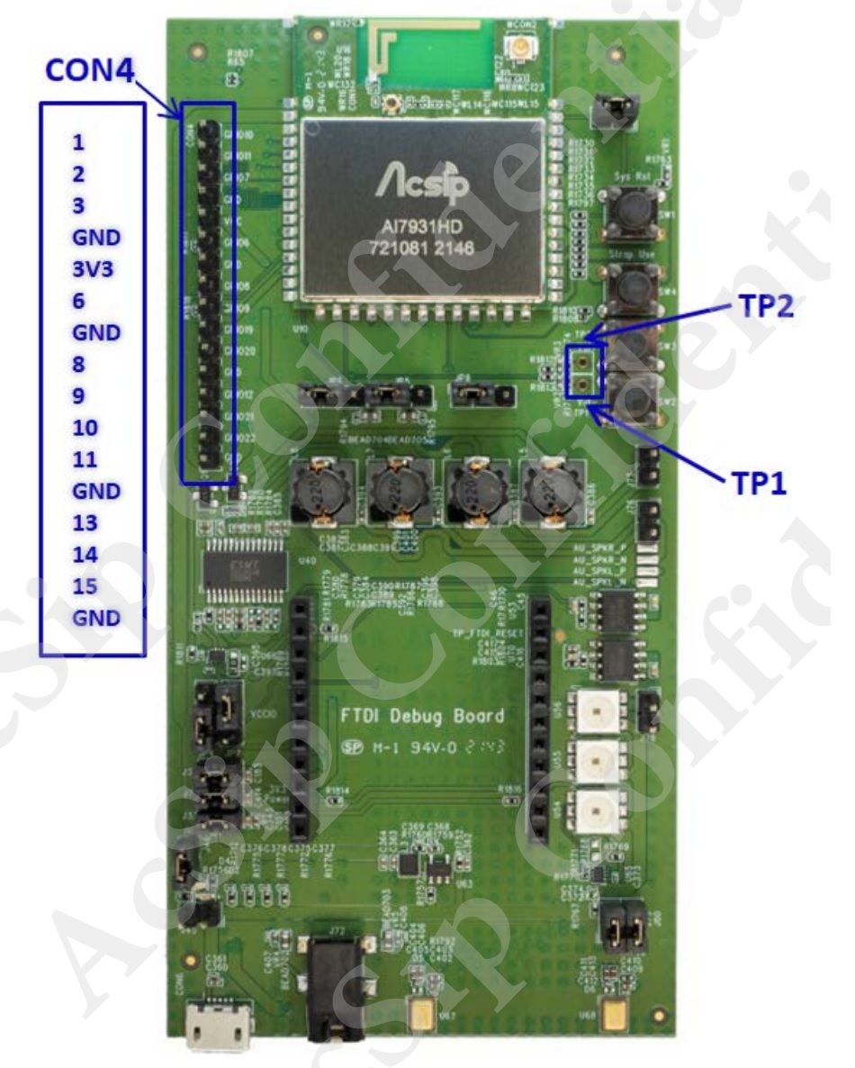
Figure 8. GPIO pin-out extension connectors
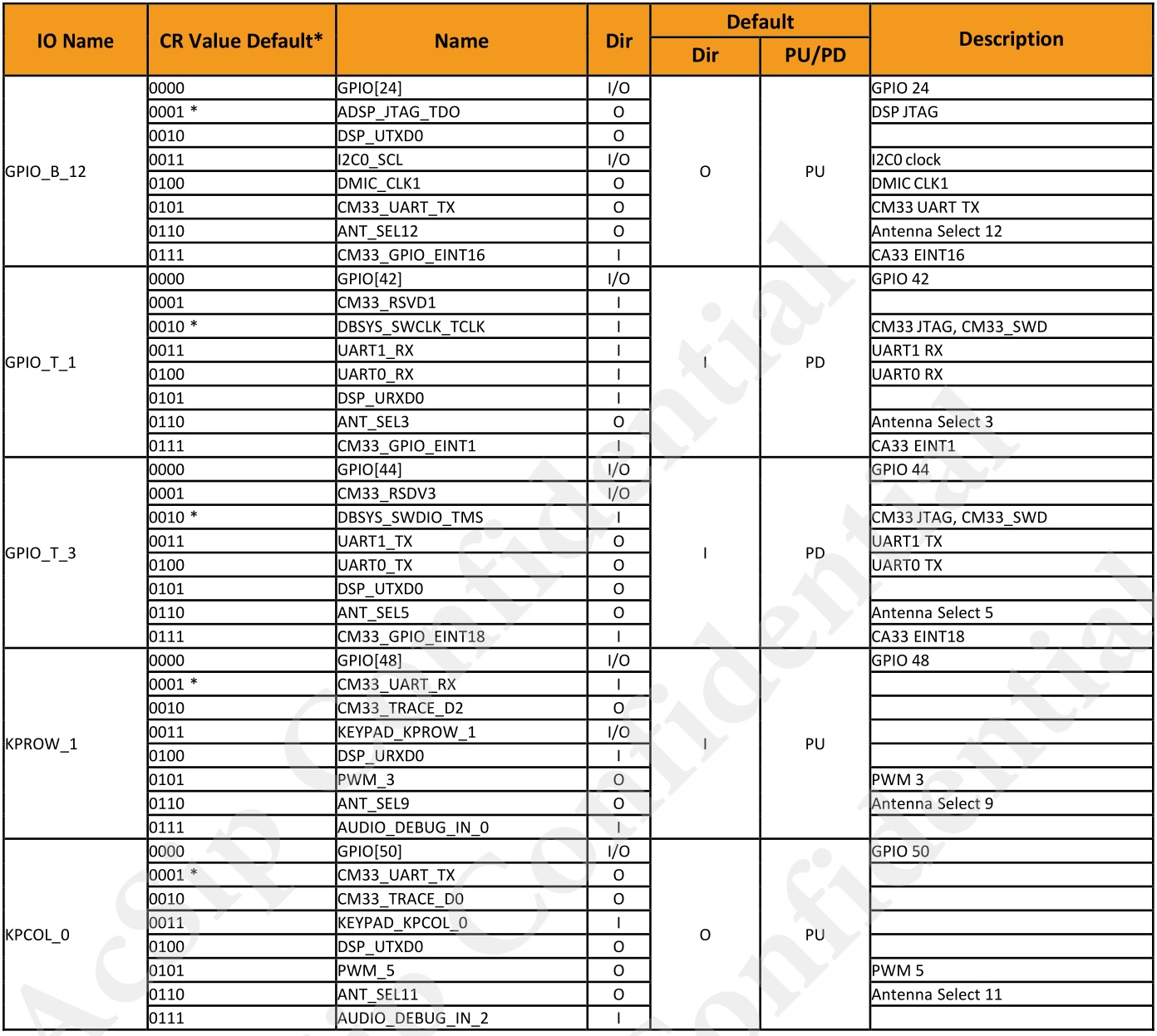
Table 4 GPIO pin-out extension connector
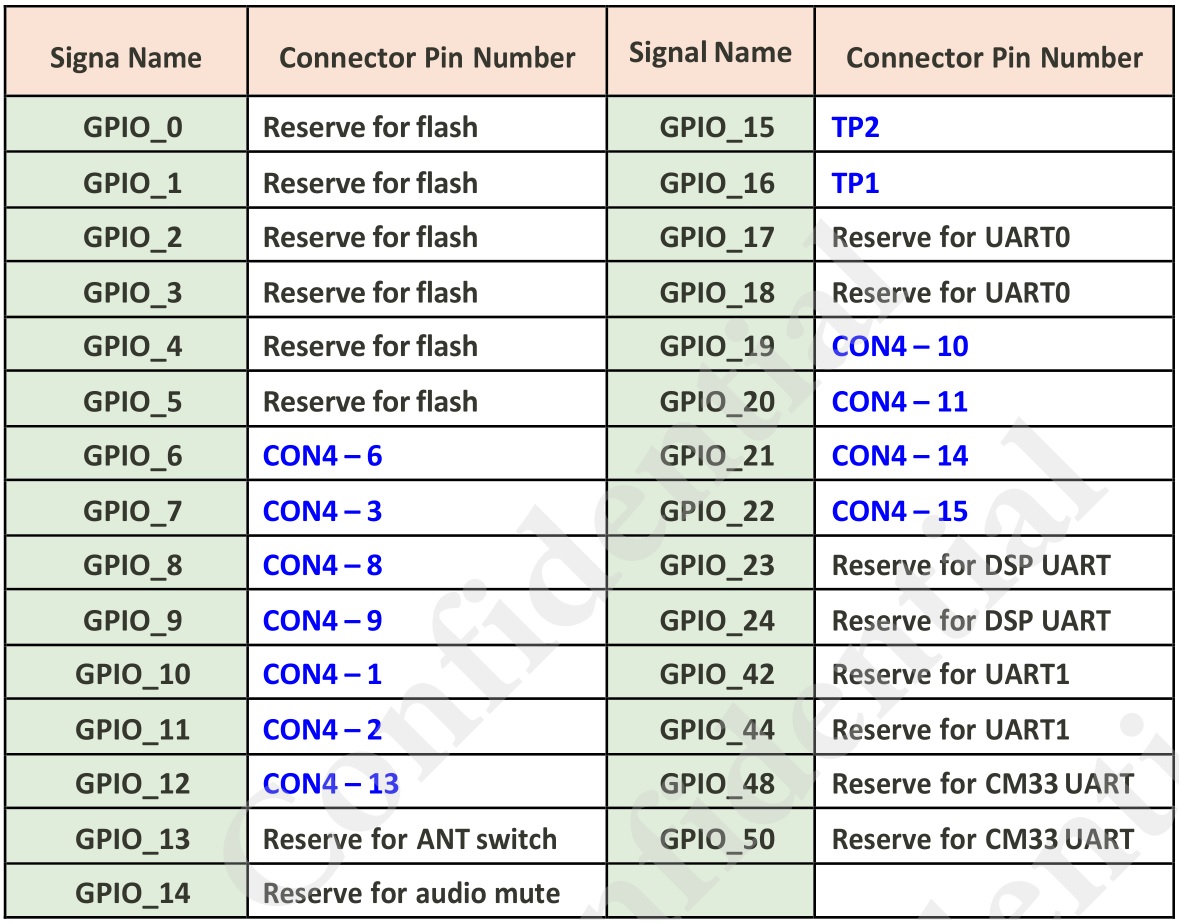
Table 5 GPIO pin multi-function definition

4.8.FTDI debug board
By default, EK-AI7931HD should plug in a FTDI debug board at U69 (Figure 9). Within this FTDI debug board (Figure 9) to make UART signal transfer to USB signal. This debug board also provide a Micro-USB connector to link to with your PC with USB cable
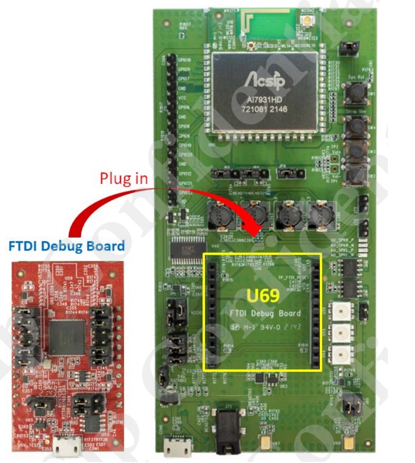
Figure 9. FTDI debug board
![]()
Product Name EK-AI7931HD
Version A
Doc No 912-13302
Date 2021/12/07
Page 20 / 20